Modelling Nanomechanical Effects in Advanced Lithographic Materials and Processes
Internally funded project
Start date : 01.09.2021


Project details
Short description
The main goal of this work is to model and simulate shrinkage and deformation effects in photoresists during lithographic processing. The finite element method (FEM) is used to model and simulate the mechanical deformation in the photoresist material and the Dr.LiTHO lithography simulator is used to simulate the optical and chemical aspects. Moreover, a machine learning implementaion is introduced which helps predict pattern collapse probabilities making use of training data generated with the help of FEM tools and Dr.LiTHO.
The research project is being worked on as part of an LEB PhD project in collaboration with the Fraunhofer Institute of Integrated Systems and Device Technology.
Scientific Abstract
The research project is being worked on as part of an LEB PhD project in collaboration with the Fraunhofer
Institute of Integrated Systems and Device Technology.

The semiconductor electronics field has come a long way in the past century and is only going to grow by leaps and bounds. The very first semiconductor device can be traced back to the rectifier (AC-DC converter)that was invented way back in 1874. The building blocks of today's semiconductor devices are the transistors and they  were invented much later in the year 1947 by Bardeen and Brattain at Bell Laboratories, USA. The semiconductor industry has evolved quite a lot since due to various advancements in technology and has transitioned to the integrated circuit (IC) era. These ICs have made their way into a wide variety of electronic products ranging from the humble calculator to electric vehicles (EVs) and also to more advanced technologies like that of a space rocket launch system. The metal-oxide-semiconductor field-effect transistor (MOSFET) is the most commonly used type of field-effect transistor (FET) that makes up current generation ICs. There can be billions of these MOSFETS on microprocessor devices such as the latest one from Apple. The wonderful field of photolithography has made it possible to manufacture these transistors that are known to be the building blocks of semiconductor devices. State-of-the-art clean rooms with very low levels of contamination and newer lithography techniques have allowed for the manufacture of semiconductors in a fewer number of steps to keep up with the demand of the industry.
The path towards achieving a large number of transistors on a chip has become quite challenging of late due to the processes employed. Smaller features require a light source with a lower wavelength, which in turn can make manufacturing difficult and less predictable. The major bottleneck in the process is now the pattern transfer from the mask to the wafer. This is mainly due to the various chemical, optical and mechanical effects taking place within the photoresist polymer. The feature shapes and contours may not always match the design specifications of the mask due to these effects. Such defects can considerably reduce the throughput of the lithographic system and lead to losses in process productivity and increase costs. Various complex correction measures are employed to help mitigate these defects. Good defect prediction models need to be developed and implemented in order to predict and understand their occurrences. Moreover, defects in modern extreme ultraviolet lithography (EUV) do not scale with the feature size. The defects can therefore be in the range of several nanometers, which make them quite large to neglect. Many of the lithographic simulators do not have the means to correctly and accurately predict all the outcomes of the numerous lithographic processes. Since lithography is a vast field encompassing a number of scientific areas ranging from optical physics, chemistry, mathematics and mechanics, modelling and simulating a complete process till the final stage can be very challenging. Compact models have been used in the past as a compromise to help balance the performance and accuracy requirements in order to suit the needs of the industry. These models however can fall short in terms of accuracy while being quite good when it comes to performance. There is therefore a need to model certain aspects of the lithographic process using rigorously models and combine them with a compact/faster model for certain processes to make a trade-off in the simulator.
Computational methods can greatly help in better understanding the impact of various process settings on the final outcome of the lithographic process. Process and parameter optimizations can be carried out without spending too much effort and time to get the results. Simulations play a key role in processes that are less deterministic in nature or are influenced by a number of different outcomes. This makes photoresist process simulation quite formidable since it is the final stage of lithographic processing and is therefore influenced by all the prior processes. To maintain pace with the growing demands of the semiconductor industry, more complex or otherwise unexplored aspects of photoresist processing need to investigated. Negative-tone development (NTD) methods in conjunction with bright field masks have become a mainstay in lithography due to various benefits with regards to image contrast and line width roughness (LWR). With the growing usage of the NTD process lithographers are being confronted with a number of challenges. Resists that are subjected to NTD are susceptible to a variety of undesirable effects like shrinkage during the post-exposure bake (PEB), deformation, variable development rates and pattern collapse. These issues need to be tackled or mitigated to help in the further progression of EUVL. A number of simulation models and algorithms need to be developed in order to correctly predict and analyse the defects encountered.
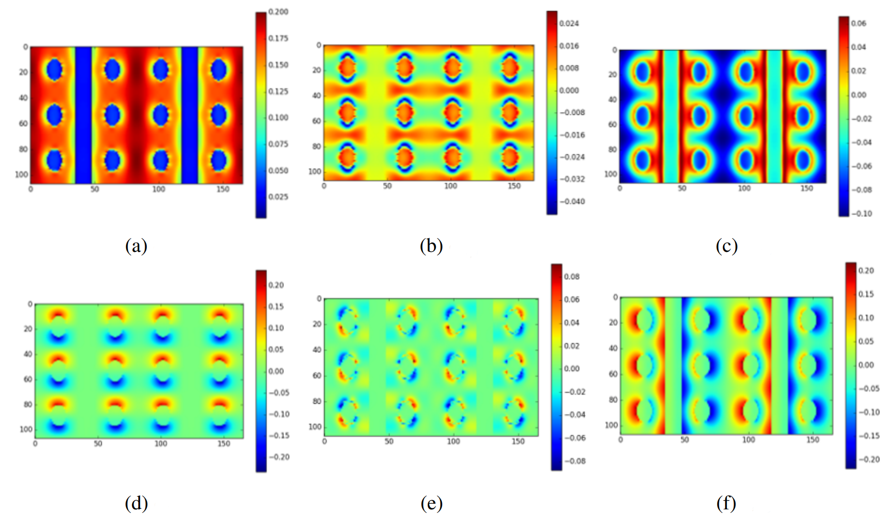
The main objective of this thesis is to model, simulate and predict a diverse set of nano-mechanical effects seen in photoresist materials. A number of photoresist effects leading to some form of deformation are observed right from the exposure step. A finite element method (FEM) based model is developed to help simulate the shrinkage and volume losses seen in NTD resists. This new model uses a relational principle where the protection group concentration is analogized with the thermal expansion coefficient during the PEB step. Additional fitting parameters like the shrink factor are then used in the model along with the crucial material properties comprising of the Young's modulus, Poisson's ratio and density. The shrinkage affects the critical dimension (CD), height and volume of the final photoresist profile greatly and is the main source of the overall dimensional disparity. The protection group concentration values along with the various light and chemical composition profiles are extracted from simulations performed using the lithography simulator Dr.LiTHO developed at Fraunhofer IISB. The results obtained from this simulator are used as an input to the more rigorous FEM deformation models developed in this thesis. The deformation during PEB also leaves a certain amount of stress and strain within the bulk of the resist which contributes to further deformation during the development step. Another model is developed to help understand this effect seen from experimental data. The standard kinetic development rate model does not capture the influence of strain on the overall development rate. A newer improved version for the development rate which incorporates the impact of strain and prior deformation is established. Strained regions could lead to localized areas with higher development rates that cause variations in CDs and profile contours. A combination of mechanical, chemical and optical proximity effects gives rise to these more complex defects in NTD resists. After development there is a change in boundary conditions, i.e. the resist material is washed away leaving behind a free-standing feature. This free-standing feature depending on the dimensions, shape and feature density can begin to gradually relax due to a gradual decrease in the residual stresses. A model simulating this behaviour is introduced to help predict the extent of sidewall angle and CD changes occurring.
After the resist undergoes a chemical development, a rinsing of the resist surface is carried out before the final etching step. The chemical developer liquid dissolves parts of the resist and can leave residues on the final pattern above the substrate. The rinse liquid (usually water) is therefore used to get rid of the residual developer present on the resist profile and keep it clear of contaminants. There is however an issue with this procedure which can lead to pattern bending and collapse. There is a possibility that the rinse liquid does not dry evenly due to the shape and layout of the overall pattern. The surface tension of the rinse liquid could in turn cause the resist pattern to collapse. The presence of an underlayer or hardmask in EUVL adds another element of risk to the stability of the pattern. Resist debonding or delamination can be induced as a result of the lack of adhesion with the underlayer. This effect along with pattern bending is modelled for the two most prominent use cases, namely lines and spaces and pillar shaped patterns. Pattern collapse in previous generation deep ultraviolet lithography (DUVL) was mainly caused due to the higher aspect ratios of the patterns which can negatively impact its mechanical stability. In EUVL however, there are a different set of reasons responsible for this problem. Resist features in EUVL however have lower aspect ratios but the material is generally much softer and can also suffer due to lower adhesion with the substrate/underlayer and line width roughness (LWR) arising due to a variety of stochastic effects. The standard model used to simulate pattern collapse in DUVL would therefore not suffice to simulate the same in EUVL. Localized regions of higher aspects ratios and higher feature densities arising from LWR can make the modelling of collapse and feature bending much more challenging. To circumvent this issue, a machine learning based approach was used and a large amount of data was generated to train a network to predict collapse probabilities for resists with varying degrees of roughness emanating due to stochastics. The rough profiles for the one-dimensional lines and spaces feature can be represented by using a combination of power spectral density (PSD) functions with parameters calibrated against experimental data.
