Thin-Film Transistors with Novel Architecture for RF Circuits and Systems (FFlexCom)
Third Party Funds Group - Sub project
Acronym: FFlexCom
Start date : 01.06.2016
End date : 30.05.2019

Overall project details
Overall project
High Frequency Flexible Bendable Electronics for Wireless Communication Systems
Project details
Short description
Short description
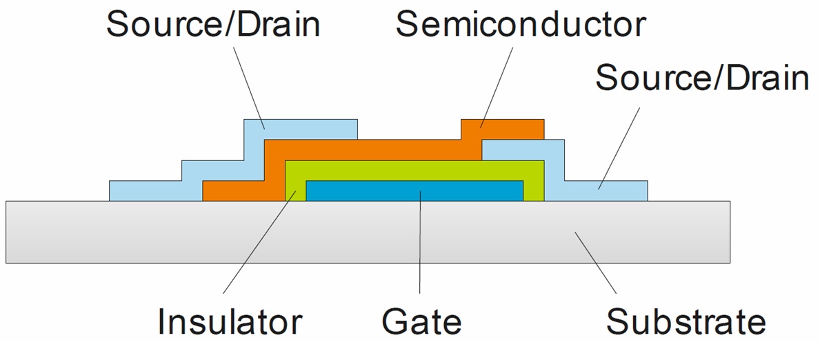
Thin-film transistors (TFTs) are mainly used in flat panel displays as switches for selecting pixels. In TFTs the electric conductivity of a semiconductor layer placed between two contacts, called source and drain, is influenced by a third contact, the gate. The current can thus be varied over several orders of magnitude. The TFT is switched off when the current flow is negligibly small (for example a few pikoampere) and switched on when the current is much larger (for example, several microampers). Switching over always takes some time (fractions of seconds). If source and drain are closer together (the so-called channel is smaller), this time is reduced and the TFT switches faster. In state of the art thin-film-transistors (TFTs), both source and drain electrodes are placed at the same side or interface of the semiconductor layer. Positioning the two contacts on opposite interfaces of the semiconductor in an Alternating Contact TFT (ACTFT) enables new degrees of freedom for device design, optimization, and operation. The ability to enable short channel lengths is explored for application in radio frequency (RF) circuitry in this project.Two research groups of FAU Erlangen Nuremberg being experts in device technology (Chair of Electron Devices) and RF circuits engineering (Institute of Electronics Engineering) join forces to cover the integrated development of ACTFTs towards basic RF building blocks and systems based on flexible metal oxide TFTs. Studies on device physics, RF behavior, and novel circuit concepts will open perspectives for the use of large area, thin, and bendable TFT technologies in future industrial, consumer, and wearable electronics.
